TSMC focuses on power and efficiency with the new 2nm process node
TSMC has just revealed its upcoming 2nm node, said to offer an up to 30% performance boost and greater power efficiency when it comes out in 2025.

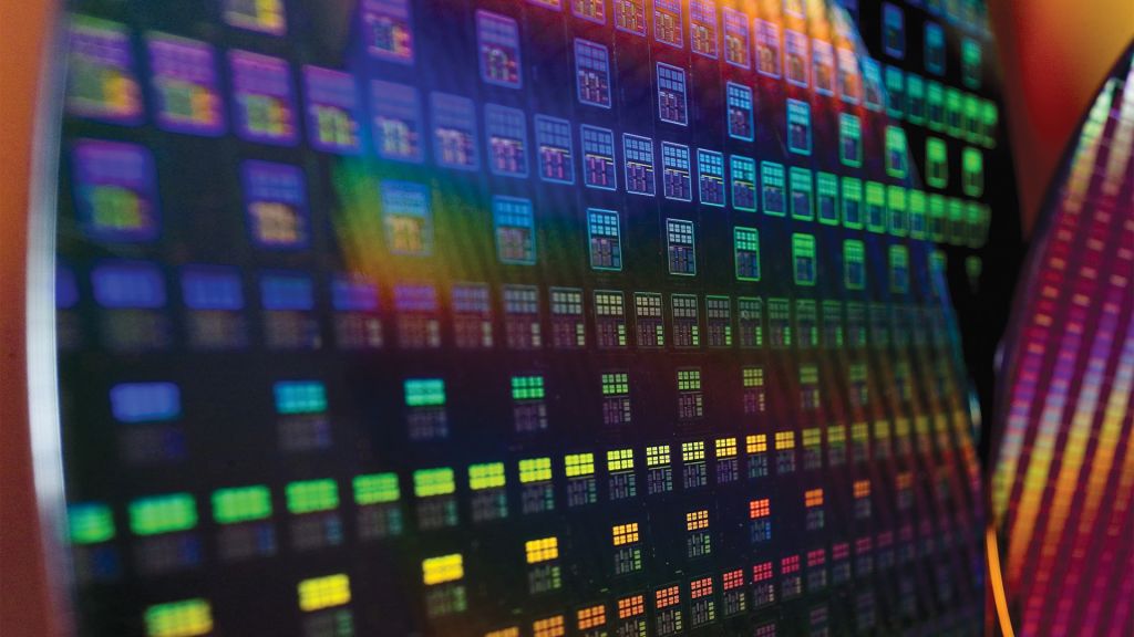
The Taiwan Semiconductor Manufacturing Co. (TSMC) has just officially unveiled its 2nm node, dubbed the N2. Set to release sometime in 2025, the new process will introduce a new manufacturing technology.
According to TSMC’s teaser, the 2nm process will either provide an uplift in pure performance compared to its predecessor, or, when used at the same power levels, will be much more power-efficient.
 TSMC
TSMCTSMC talked about the new 2N technology at great length, explaining the inner workings of its architecture. The 2N is going to be TSMC’s first node to use gate-all-around field-effect transistors (GAAFETs) and will increase the chip density over the N3E node by 1.1 times. Before the 2N is ever released, TSMC will launch 3nm chips, which have also been teased at the 2022 TSMC Technology Symposium.
The 3nm node is going to come in five different tiers, and with each new release, the transistor count will go up, therefore increasing the chip’s performance and efficiency. Starting with the N3, TSMC will later release the N3E (Enhanced), N3P (Performance Enhanced), N3S (Density Enhanced), and lastly, the “Ultra-High Performance” N3X. The first 3nm chips are said to hit launch in the second half of this year.
While the 3nm process is nearer to us in terms of the launch date, it’s the 2nm that’s slightly more interesting, even though it’s still a couple of years away. TSMC’s goal with the 2nm node seems to be clear — increasing the performance-per-watt to enable both higher levels of output and efficiency. The architecture as a whole has a lot to recommend it. Let’s take the GAA nanosheet transistors as an example. They have channels surrounded by gates on all sides. This will reduce leakage, but the channels can also be widened, and that brings a performance boost. Alternatively, the channels can be shrunk to optimize the power cost.
Both the N3 and the N2 will offer considerable performance increases compared to the current N5, and all of them give the choice of balancing power consumption with performance-per-watt. As an example (first shared by Tom’s Hardware), comparing the N3 to the N5 nets an up to 15% gain in raw performance, and an up to 30% power reduction when used at the same frequency. The N3E will bring those numbers even further, up to 18% and 34%, respectively.
 TSMC
TSMCNow, the N2 is where things start to get exciting. We can expect to see an up to 15% performance boost when used at the same power draw as the N3E node, and if the frequency is brought down to the levels provided by the N3E, the N2 will deliver an up to 30% lower power consumption.
Where will the N2 be used? It will likely find its way into all kinds of chips, ranging from mobile system-on-a-chips (SoCs), advanced graphics cards, and equally advanced processors. TSMC has mentioned that one of the features of the 2nm process is “chiplet integration.” This implies that many manufacturers may use the N2 to utilize multi-chiplet packages to pack even more power into their chips.
Smaller process nodes are never a bad thing. The N2, once it’s here, will deliver high performance to all manner of hardware, including the best CPUs and GPUs, while optimizing the power consumption and thermals. However, until that happens, we’ll have to wait. TSMC won’t start mass production until 2025, so realistically, we are unlikely to see 2nm-based devices entering the market before 2026.

 Fransebas


