I got a rare peek into Intel’s largest offshore manufacturing facility — here’s what I learned
Intel gave us access to its biggest offshore facility located in Malaysia to show us how it manufactures CPUs.

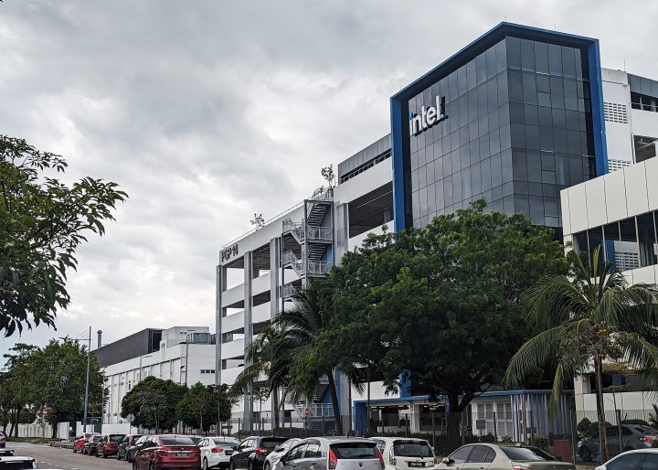 Kunal Khullar / Digital Trends
It is rare to see a technology giant open its doors to showcase how it really operates. But that is exactly what Intel had in mind when it invited global press and media representatives to visit its factories in Malaysia. As a part of its Tech Tour 2023 event, the chip maker gave us a detailed insight into how exactly a CPU is made. I learned a lot, but before I share my experience, here’s a brief about the company’s history and future plans in Malaysia.
Intel established its first offshore facility in Malaysia in 1972 with a total of 100 employees. Today, there are two major facilities in Penang and Kulim that expand close to 900,000 sq. ft. with 15,000 employees.
 Intel
IntelWith growing demands, and to keep up with its IDM 2.0 strategy, Intel is already expanding the coverage of its facilities. A new advanced packaging facility called Pelican and an assembly test facility called Falcon are currently under construction and are expected to be operational in the coming two years. The company has also envisioned a total of 7 million square feet built-up area, with over 2 million sq. ft. manufacturing space all expanded over 16 buildings in the future.
Visiting Intel Malaysia
The tour was split into two days where we first visited the the Penang Assembly and Test (PGAT) facility. This is where the silicon dies are assembled, validated, and tested for errors. But it is the Kulim facility where the magic begins. The Intel Kulim Die Sort Die Prep or KMDSDP is a state-of-the-art facility for processing silicon wafers, the raw material that makes up the best processors.
This factory receives the silicon wafers from fabrication plants, conducts die preparation processes, and subsequently categorizes them for package assembly and testing at various Intel assembly/test facilities around the world. The KMDSDP facility is located on the mainland, unlike the Penang facility which is on the island itself, which meant a longer bus ride crossing a gorgeous-looking bridge over the sea.
 Intel
IntelOnce we reached Kulim, we were given a brief and were asked to wear special bunny suits with additional headgear and beard protection before we could step in. This was necessary as the manufacturing areas are meant to be dust-proof. Of course, that also meant we were not allowed to carry anything inside including phones, cameras, or other recording equipment.
Die prep, die sort
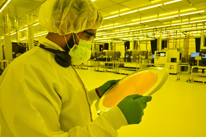 A look at an entire silicon wafer that is stuck onto a mylar sheet Intel
The KMDSDP facility is responsible for two main operations – die preparation and die sort. In the die preparation phase, complete 300mm wafers are received from the fabrication facilities and attached to a flexible mylar. These are semi-transparent sheets and are necessary to ensure that each die stays in position after it has been cut and separated.
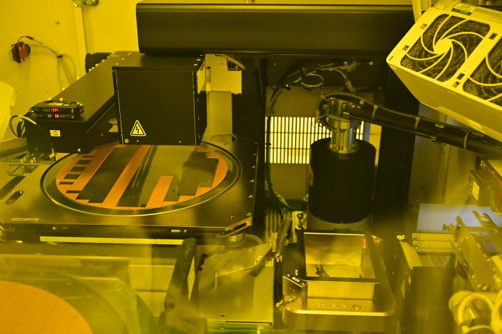 A fully automated machine cuts individual CPU dies from an entire piece of wafer Intel
Depending on the type of processor, these wafer sheets go through multiple processes including grinding, laser scribing, and mechanical cutting to create individual chips. Next, using a special vacuum and UV light combination, the chips are separated from the mylar. These individual chips are then placed into trays using robotic arms and are slotted into larger plastic boxes before carrying them to the subsequent sorting operation.
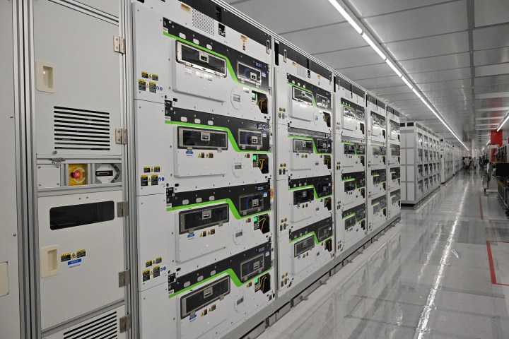 A sorting module with various test cells Intel
Next, each of these chips undergo testing to identify any defects and are sorted at the same time. To accomplish this, Intel uses massive sorting modules which are as big as a bus having a total of 20 individual test cells. Each test cell weighs approximately 1,000 pounds, and to maneuver these, there is a specially designed lifting mechanism that hovers above the floor using a cushion of air just like a hovercraft. It felt almost magical to move this gigantic piece of transport with just one hand.
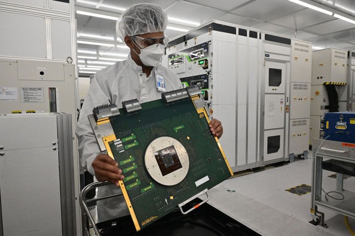 An inside look at a test cell that goes into a sorting module Image used with permission by copyright holder
Trays are loaded on one end and are then distributed among various test cells. Since each test cell operates independently, workers can access a test cell from a sorting module for maintenance purposes. Each chip is tested using a probe card equipped with thousands of fine needles, thinner than a human hair, which connects to the integrated circuit within the testing equipment. This probe card measures the electrical characteristics of the chip circuits to evaluate reliability and identify defects. All of the testing is done automatically while a worker keeps an eye on the entire process using various monitors.
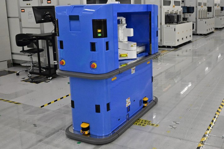 One of the many automated guidance vehicles (AGVs) in action Intel
There were also some special automated guidance vehicles (AGVs) that caught everyone’s attention primarily due to their ice cream truck-like tone. Their main task is to handle the movement of lots between the storage spaces and the test equipment. They require almost zero human intervention and hover around the facility along dedicated paths.
Once a tray has finished going through the test and characterization phase, they are returned to the area where the wafer was cut into individual chips. The chips that do not pass the testing phase are collected separately and are either discarded or recycled. The trays with chips that have successfully passed all testing are sorted and assigned to a certain SKU (Core i9, Core i7, etc.). Each chip is taken out of the tray and sealed between two layers of film which are then rolled onto a reel, so they can be transported to the Assembly and Test facilities situated around the globe, for further processing.
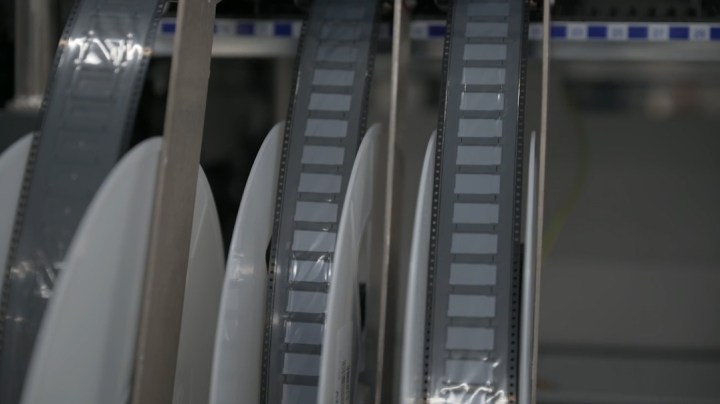 Individual CPU dies are packed inside reels Intel
On to assembly and testing
The next part of the tour included a visit to the Penang Assembly and Test (PGAT) facility, which is situated on Penang Island. This manufacturing facility focuses on assembling and testing various chips by the millions every day. Essentially all the reels are received at this facility, and then each die is removed, packaged, and tested before they are ready to hit the stores.
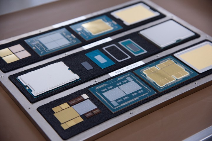 An overview of the Advanced Packaging process showing various dies, substrates, and IHS Intel
The assembly and test process at PGAT has six key stages. It all begins with the Chip Attach process where the die or the chip is attached to the substrate — the base material of the CPU. This is done using the Foveros face-to-face (F2F) chip-on-chip bonding process which was first introduced in 2019. The process requires a high amount of precision as any imperfections can cause severe damage to the chip. An additional layer of epoxy underfill is applied evenly to remove any microscopic gaps between the die and the substrate.
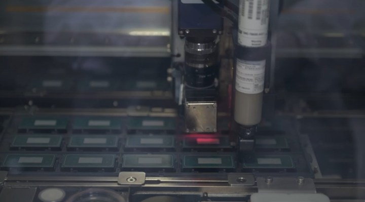 A machine applies adhesive over the substrate before the IHS is fixed on top of the dies Intel
The next step is to attach the Integrated Heat Spreader (IHS) or the lid of the CPU. This helps in efficient heat dissipation in end-user systems. A machine is used to first apply a certain amount of thermal interface material to the die, followed by the adhesive so that the IHS lid can be put in place. We now have a finished product that is ready for action. But before that, it has to go through some rigorous testing.
Once the CPU is ready, it has to go through various tests to ensure that the product works as intended. This is done at the Design And Development Lab at PG16 in Penang.
First up is the burn-in test during which Intel exposes the chips to high temperatures and voltages to identify and eliminate any defects. Chips that successfully pass this test then proceed to electrical testing, which includes testing of all electrical traces and as well as functionality. Finally, the chips have to go through the PPV testing phase which is to validate platform product screening to confirm functionality in actual customer computer systems running Windows, Linux, or other operating system environments. Essentially it is a process that mimics a customer environment and additionally tests various aspects like memory, PCIe lanes, etc.
The final stage of the tour included a visit to the System Integration and Manufacturing Services (SIMS), a special factory that manufactures equipment to test and validate CPUs during their production. Not only does this facility make testing equipment for Intel Malaysia, but also ships them to various other Intel facilities around the world.
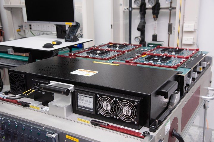 An HDBI tester Intel
We had a chance to check out some of the testing equipment including the High Density Burn-In (HDBI) tester, the High Density Modular Tester (HDMT) tester, and the System Level Tester (SLT). The HDBI tester is used to perform burn-in stress testing on high temperature and voltage on Intel CPUs while the HDMT provides the capability to perform class or backend testing. Intel says that this tester is used in their factories and labs for new product development and CPU production ramping. Lastly, the SLT is used to confirm Intel products will function in a customer-like environment. Every tester is designed to align with the features and precise requirements of the CPU, guaranteeing sufficient test coverage and, maintaining product quality.
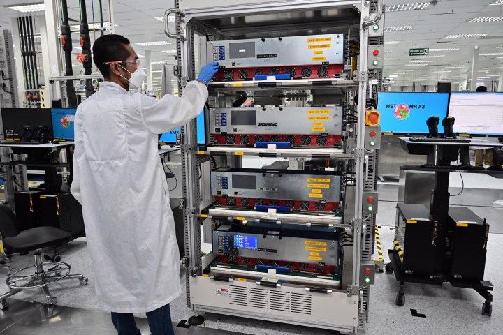 A stack of testing equipment at Intel’s SIMS facility Intel
An unparalleled experience
The entire experience of witnessing and comprehending the CPU manufacturing process was genuinely unparalleled. I was absolutely impressed by the immense scale of operations and the intricacies involved in producing a single unit of the final product. The entire manufacturing facility functions like a well-oiled machine, yet it is underpinned by various complexities and tireless dedication of the company’s workforce.
Navigating through various sections of the manufacturing facilities not only provided me with a deeper understanding of how the company crafts its top-tier chips but also offered a clear glimpse into Intel’s future. Its commitment to introducing five nodes within the next four years may appear as a marketing strategy, but it seems entirely feasible, especially given the impressive capabilities of its manufacturing plants. These plants also ensure that the company is on track with its IDM 2.0 strategy for manufacturing, innovation, and product leadership.
 Intel
IntelHowever, it’s important to recognize that Intel won’t have an unobstructed path to success. There’s fierce competition from rivals like AMD and other chip manufacturers, and only time will reveal whether Team Blue can maintain its leadership in the industry.
For now, we are expecting Intel to launch new mobile chipsets later this year under the 14th-gen ‘Meteor Lake’ moniker. It is expected to be an important milestone for the company as it will employ the Intel 4 process making it the first chip lineup to utilize the 7nm process. Soon after that, there are rumors that the next-gen desktop processors will also be arriving as a refresh to the existing 13th-gen Raptor Lake lineup.

 Tfoso
Tfoso 


